


-- New generation Toshiba BiCS FLASH™ adds layers, boosts capacity --
TOKYO — (BUSINESS WIRE) — July 26, 2016 — Toshiba Corporation (TOKYO: 6502) today unveiled the latest generation of its BiCS FLASH™ three-dimensional (3D) flash memory with a stacked cell structure*1, a 64-layer device that will be first*2 in the world to start sample shipments today. The new device incorporates 3-bit-per-cell (triple-level cell, TLC) technology and achieves a 256-gigabit (32-gigabytes) capacity, an advance that underscores the potential of Toshiba’s proprietary architecture. Toshiba continues to refine BiCS FLASH™, and the next milestone on the development roadmap is a 512-gigabit (64-gigabytes) device, also with 64 layers.
This Smart News Release features multimedia. View the full release here: http://www.businesswire.com/news/home/20160726006618/en/
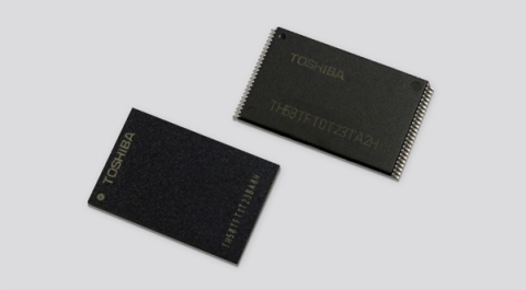
64-layer BiCS FLASH (Photo: Business Wire)
The new device succeeds the 48-layer BiCS FLASH™, and its leading-edge 64-layer stacking process realizes a 40% larger capacity per unit chip size than 48-layer stacking process, reduces the cost per bit, and increases the manufacturability of memory capacity per one silicon wafer. 64-layer BiCS FLASH™ can meet demanding performance specs, and the new device will be used in applications that include enterprise and consumer SSD, smartphones, tablets and memory cards.
Since announcing the world’s first*3 prototype 3D flash memory technology in June 2007, Toshiba has continued to advance development. The company is actively promoting BiCS FLASH™ to meet demand for larger capacity with smaller size.
Toshiba will produce the new 64-layer BiCS FLASH™ in the New Fab 2 at Yokkaichi Operations, which was officially opened earlier this month, and mass production of 64-layer BiCS FLASH™ is scheduled to start in the first half of 2017.
*1: A structure stacking Flash memory cells vertically on a silicon
substrate to realize significant density improvements over planar NAND
Flash memory, where cells are formed on the silicon substrate.
*2:
As of July 27, 2016. Toshiba survey.
*3: Toshiba presentation, June
12, 2007.
* BiCS FLASH is a trademark of Toshiba Corporation.
About Toshiba
Toshiba Corporation, a Fortune Global 500 company, channels world-class capabilities in advanced electronic and electrical product and systems into three focus business fields: Energy that sustains everyday life, that is cleaner and safer; Infrastructure that sustains quality of life; and Storage that sustains the advanced information society. Guided by the principles of The Basic Commitment of the Toshiba Group, “Committed to People, Committed to the Future”, Toshiba promotes global operations and is contributing to the realization of a world where generations to come can live better lives.
Founded in Tokyo in 1875, today’s Toshiba is at the heart of a global
network of 550 consolidated companies employing 188,000 people
worldwide, with annual sales surpassing 5.6 trillion yen (US$50
billion). (As of March 31, 2016.)
To find out more about Toshiba,
visit
www.toshiba.co.jp/index.htm
View source version on businesswire.com: http://www.businesswire.com/news/home/20160726006618/en/
Contact:
Toshiba Corporation
Storage & Electronic Devices Solutions Company
Koichi
Tanaka / Kota Yamaji
Communications & IR Group
Business
Planning Division
Phone: +81-3-3457-3576
Email Contact


 Animation, 3D Art and 3D Models")