


Announcement marks Cadence’s expansion into fast-growing system analysis and design market
Highlights:
- The first product in Cadence’s system analysis initiative, the Clarity 3D Solver delivers up to 10X faster performance for electromagnetic simulation with virtually unlimited capacity and gold-standard accuracy
- New breakthrough architecture can run on hundreds of CPUs optimized for both cloud and on-premises distributed computing
- True 3D model extraction eliminates risk from manually reducing the size of structures being modeled
- Easily reads design data from all standard chip and IC package platforms and offers unique integration with Cadence implementation platforms
SAN JOSE, Calif. — (BUSINESS WIRE) — April 2, 2019 — Cadence Design Systems, Inc. (NASDAQ: CDNS) today entered the fast-growing system analysis and design market with the announcement of the Cadence® Clarity™ 3D Solver, which delivers gold-standard accuracy with up to 10X faster simulation performance and unbounded capacity compared to legacy field solver technology. Harnessing state-of-the-art distributed multiprocessing technology, the Clarity 3D Solver efficiently tackles electromagnetic (EM) challenges encountered when designing complex 3D structures on chips, packages, PCBs, connectors and cables—bringing true 3D analysis to any engineer with desktop, high-performance computing (HPC) or cloud computing resources. The Clarity 3D Solver easily reads design data from all standard chip, IC package and PCB implementation platforms while also providing unique integration benefits for design teams using the Cadence Allegro® and Virtuoso® implementation platforms. For more information, please visit www.cadence.com/go/3dsolver.
This press release features multimedia. View the full release here: https://www.businesswire.com/news/home/20190402005280/en/
The Cadence Clarity™ 3D Solver efficiently tackles electromagnetic challenges encountered when designing complex 3D structures on chips, packages, PCBs, connectors and cables—bringing true 3D analysis to any engineer with desktop, HPC or cloud computing resources. (Graphic: Business Wire)
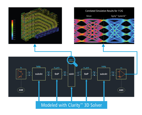
Highly complex structures found in silicon interposers, rigid-flex PCBs and stacked-die IC packages must be modeled accurately in 3D for structure optimization and high-speed signaling compliance. High-speed signaling, such as in 112G serializer/deserializer (SerDes) interfaces, relies on high-fidelity interconnect design. Any slight change in impedance can negatively impact bit error rate, so optimization entails extensive research including dozens of complex extractions and simulations. To accommodate this workload, legacy field solvers must run on massive, expensive high-performance servers. In addition, speed and capacity limitations of legacy field solver technology require users to carefully simplify and/or partition the structure into smaller segments to fit within local computing constraints. This pseudo-3D approach creates the risk that the resulting final model may contain inaccuracies due to artificial effects from the superficial model boundaries.
Clarity 3D Solver technology addresses the most complex EM challenges faced when designing systems for 5G communications, automotive/ADAS, HPC and IoT applications. Industry-leading Cadence distributed multiprocessing technology enables the Clarity 3D Solver to deliver virtually unlimited capacity and a 10X speed up required to efficiently and effectively address these larger and more complex structures. The Clarity 3D Solver creates highly accurate S-parameter models for use in signal integrity (SI), power integrity (PI) and electromagnetic compatibility (EMC) analysis, enabling simulation results that match lab measurement.
The Clarity 3D Solver is optimized to distribute a job across multiple low-cost computers while remaining equally efficient when running on a more powerful and expensive server with terabytes of memory. A unique distributed adaptive meshing approach and significantly smaller memory requirements than legacy 3D field solvers enable the Clarity 3D Solver to extensively utilize cost-effective cloud and on-premises distributed computing. These advantages make the cloud-ready Clarity 3D Solver an ideal choice to optimize a company’s cloud computing budget.
Using the Clarity 3D Solver in conjunction with the Cadence Sigrity™ 3D Workbench, users can merge mechanical structures such as cables and connectors with their system design and model the electrical-mechanical interconnect as a single model. The Clarity 3D Solver is also tightly integrated with the Virtuoso, Cadence SiP Layout and Allegro implementation platforms, enabling 3D structures to be designed in the Allegro and Virtuoso environments, optimized in the analysis tool and implemented in the design tool without being redrawn.
“At gigabit speeds on our highly dense PCBs with over 30 layers, we
depend on accurate interconnect extraction of our complex structures to
support signal integrity analysis,” said Rick Burns, vice president of
engineering, Semiconductor Test Division at Teradyne. “With the Cadence
Clarity 3D Solver, we can achieve the necessary accuracy in a fraction
of the time it has previously taken. This has opened up a new era of
analysis possibilities for us since we can now run dozens of simulations
in the time it has previously taken to run one. This reduces design
re-spins and helps us fulfill our promise of delivering the highest
throughput and lowest cost of test for our customers.”


 Animation, 3D Art and 3D Models")