Introduction
Last Edit July 22, 2001
Introduction to Chapter 1
Application-Specific Integrated Circuits (ASIC) [1996]
Application-specific integrated circuits (ASICs) fit between the detailed
full-custom circuit designs and the off-the-shelf pre-designed components.
They offer the designer a faster method of tailoring the circuit to the
task while retaining most of the fast design turn-around time offered
by predesigned parts.
The Array
An ASIC array is a single die from a production wafer. in the 1990s,
it was generally two or three layers of metalization placed on top of
a base array. Figure 1-1 provides an overview of the steps involved in
building a semi-custom array.
By 2001, the levels of metalization had climbed to an average of six
layers of metalization. At least two layers are usually reserved for power-ground
planes. THe layers in the base array varied with the process with 26-28
layers in the base die being a reasonable assumption.
Figure 1-1 Semicustom Array Processing
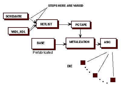
The base array is predesigned by the array vendor. It consists of the
layers required to define the cells and the components within them. These
components vary depending on the type of cell and the array family. They
are resistors, diodes, transistors (bipolar or CMOS) with capacitance
and impendances implied in the layering. The threshold voltage generators
and other overhead circuitry will also be included in the base design.
| WAFER -----------------> |
DIE |
| multiple die |
Individual array |
The array designer will have already determined where the fixed power
and ground pads are located, how many types and how many of each type
of cell there is per array, and what design rules are required in the
use of the array. The base array is pre-manufactured, reducing the turn-around
time of the design between design acceptance and prototype or production.
CBA Design System designers had the priveledge of designing their own
base die, including punch-outs for hard IP blocks, and power-ground routing
for RAMs and soft IPs.
The wafer is put through wafer-sort to determine good and bad die. The
die is a pre-packaged part which can be and is tested. When packaging
is completed, the packaged part is retested.
Wafer verification software (Dracula comes to mind) must verify all layers
of the wafer, metalization and the base die, and verify that all IP blocks
and memory blocks are properly connected. Hard IP blocks interconnect
or "stitch" into all levels of the base die.
Customization
The customization of the array comes from the interconnect of the base
array components. The interconnect is both the intraconnect between
components within a cell to form a function, called a macro, and the interconnect
between the macros to form the circuit module. One or more modules may
be placed on an array.
The interconnect between macros is considered the routing or nets. Routability
is a measure of the ability to transform the design to physical metal
etch patterns or the metalization of the array. The macros are formed
by a predefined layout pattern that is not considered part of the routing
problem.
Macros may exist with several "footprints", which allow them
to be positioned with different layout aspects. They also exist in different
drive versions, which may also cause differences inthe layout pattern.
Switching a macro from one drive configuration to another may require
its relocation in the circuit layout.
With the high-speed arrays already available, the time delay or propagation
delay through an interconnect net under heavy loading conditions may exceed
the propagation delay through a macro. Priority pre-placement, design
optimization for speed and other design approaches must be used to control
the interconnect delays.
For DSM technologies, any technology below 0.18
micron, it is given that the interconnect delays will represent
approximately 70% or more of the timing path delay
|
These tehnologies require pro-active design methodologies to be successful.
Design partitioning, placement, and careful constraints are all required
for a successful DSM design,
|
