|
Hard IP, an introduction
There is a German saying and a song that says a shoemaker should stick to his craft, which he obviously does very well, instead of trying to live the life of a Bohemian. Of course, it sounds great in German and loses everything in translation. It is the German version of the English saying: Do what you do well and stay focused. Applied to the subject at hand, there is no point for either Hard IP migration or Soft IP reuse to diminish the other's value. The key is focus: Soft IP and synthesis for the front-end, Hard IP and compaction for the back-end. In fact, Hard IP migration and Soft IP reuse are very complementary! Each discipline should focus on its strengths and on working synergistically together. The result will be a higher performance chip, reaching the market faster and less expensively, with a smiling customer at the receiving end. There have been some heated discussions about the virtue of Soft IP versus Hard IP reuse. Usually, the Hard IP side loses because the world today focuses on synthesis and Hard IP reuse is more of a niche solution. And, not to be overlooked, infrastructures in companies are set up for synthesis, not Hard IP reuse with optimization. But as always, where there is debate, even if lopsided, both sides have some valid arguments. Otherwise, it would not come to debate in the first place. In the discussion to follow, we will see that Soft IP reuse and Hard IP related techniques are synergistic. Starting out at the functional level in a top-down approach, the design process eventually evolves towards using actual components that can be associated with physical implementation. However, even if placement and route are as good as possible, choosing the perfect dimension for a transistor or the perfect size of interconnect is difficult at this point in the design process. It is easier to pick the best estimate and then later, after the first-order layout is done, use compaction to optimize to the best dimensions of devices and interconnects. From this point of view, it becomes quite obvious that back-end layout manipulations in the form of compaction are very synergistic with the front-end. What about the convenience and ease with which timing can be adjusted with compaction? How else would timing be adjusted at the back-end anyway? Rerouting would be too drastic and it could dramatically change the timing of parts of the chip that were OK before rerouting. Changing the floorplan would be even much more drastic. Adjusting transistors and interconnect sizes is a graceful and effective way to make such adjustments. Another important aspect is what we suggested in Chapter 2, when we discussed substituting poly for metal with weighting functions in compaction, as shown in Figure 2.13. There, we proposed an adjustment of the resistance between two points on a chip by varying how much of this interconnect is poly or a diffusion instead of metal. This is a neat on-chip trimming mechanism that can be done with compaction. Other trade-offs such as adjustments in resistor lengths, capacitor areas and source/drain adjustments are possible. In fact, any adjustments that are also possible by moving any polygon edges within the available space should be used to achieve the desired performance adjustments. Large percentage changes in timing can be achieved in this way. Of course, it has to be part of layout planning in the first place. In summary, there is generally quite a lot of room for performance optimization. The back-end layout manipulations are rather complementary to the front-end. In other words, if there is a timing problem in a particular path, just “massaging” the layout geometries of the transistors and interconnects for a critical path for which the timing is off may have sufficient effect on circuit timing. Accordingly, a timing problem can be eliminated without a more drastic change in the circuit. This is also particularly useful for Hard IP migration where only physical layout parameters can be manipulated. So far, all the discussions have been qualitative. As previously mentioned, intuition would suggest that only minute improvements can be achieved with back-end adjustments. Later in this chapter, we will show that this is not the case. However, before we can do this, we have to discuss the techniques with which performance is analyzed in a DSM VLSI chip to see which layout geometries need to be adjusted for optimal performance. 3.3 THE MODELING OF INTERCONNECTS
With the big influence of interconnects on circuit performance, their electrical behavior has to be adequately modeled. If we want to optimize the layout with respect to interconnects, we need to know which geometrical features to adjust and how. To determine this, we have to take a small detour into the world of interconnect modeling. To “adequately” model interconnects, we need to find a good compromise between sufficient accuracy and computational complexity. As we can see in Figure 3.2, an interconnect is not just a simple discrete circuit but, actually, a distributed load, more like a transmission line. For interconnects in today's VLSI chips, the series resistance of the interconnect normally dominates the inductive component. In the following discussions, we will assume this to be the case and will focus on capacitive and resistive effects only. This will be adequate for now. The issue of a distributed load as opposed to a simple RC network will be discussed when we examine timing analysis. Figure 3.2 shows the partitioning of the signal transport through the active parts, the buffers, and the passive parts, the interconnects. The illustration does not show where the capacitive components that determine the signal propagation along interconnects come from.
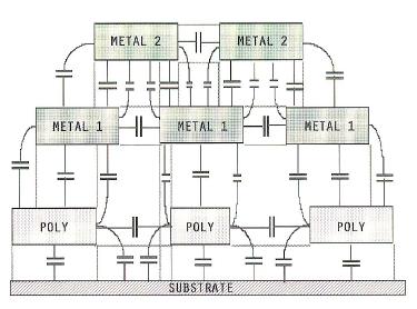
Fig. 3.2 Partitioning a Circuit into Active Parts and Interconnects Of course, to examine layout optimization, we need to look at a cross section perpendicular to the interconnect. A typical structure with all or at least the most significant interconnects surrounding and influencing the behavior of the interconnect is depicted in Figure 3.3. This is quite a realistic illustration of an interconnect structure. It is a cross section of a possible geometrical arrangement of interconnects in a multilayer metal chip. It is capacitances like the ones shown in Figure 3.3 that we have to determine. Again, we can already sense the need for approximations. The model needed is an electrical representation of interconnects to allow a simulation of electrical behavior. This electrical model has to act electrically as the actual interconnect does, within a certain degree of accuracy and a certain range of validity. For cross-sectional geometry similar to Figure 3.3, we now discuss how to determine capacitances and resistances.
Fig. 3.3 A Cross Section of a Typical Interconnect Structure Once we have found the parasitic elements for the interconnects, we will explore two aspects that, although related, serve different needs:
Ever since the DSM “scare” the problem of interconnects has received a lot of attention. For now, we are focusing mainly on digital circuits, and the digital VLSI world has for quite some time been dominated by the microprocessor. As everybody knows, speed is one of the key microprocessor selling points, and delay is the key parameter for speed. As layout geometries kept shrinking, interconnect delays became a critical issue long before signal integrity became critical. Much of the focus on interconnects was on delay models as opposed to signal integrity models. As we will see later, this need to determine the delays accurately, favored certain approximations unsuitable for signal integrity issues.
|
|||||||
|
|
|||||||
|
|||||||


 Animation, 3D Art and 3D Models")