|
CHAPTER 3
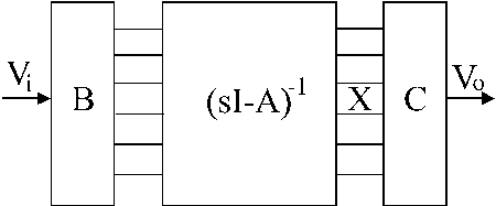
Power considerations in sub-micron digital CMOS 3.6. Power estimations in continuous time filters In the context of high frequency applications continuous time filters have an advantage over sampled data filters when power consumption is the important issue [30], [31], [32]. Apart from power overhead from clock circuitry, we need expensive amplifiers with large GBW compared to the sampling frequency for good settling behavior. There are many ways to realize a filter. In the video frequency range and above, the most employed methods are the cascades of biquads and first order sections, gyrator based filters and leapfrog simulation of ladders. Power estimations in gyrator based filters have been addressed in [28] and [29]. DR and power estimations for integrator based designs have been addressed in [7] where only the power of the output stage of the active part has been considered. In this section power estimations in cascade approach and leapfrog simulation of ladders approach are presented. The power involved in this estimations is the power needed for biasing of the complete active part. High end applications require class A operation for low distortion figures. In the following estimations, we will confine the analysis to this requirement. The estimation of power is based on DR optimization presented in [7]. Therefore, the starting point is an already DR optimized structure following the procedure from the same reference. In the state-space representation a n order filter consists of n integrators [38] and the state equations of the filter seen as a state space system are:
In (3.78), A,B,C,D are matrices, D is a scalar, Vi and V0 are the input and output variables. Fig.3.17 shows the state-space representation of the filter without considering the scalar D. The transfer function of the filter is computed from:
The eigenvalues of the matrix A are the poles of the filter. Besides, the elements of the state matrix A are related to important parameters of the filter like the input power spectral densities of the noise at the input of every integrator.
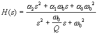
3.6.1. Power estimations for a high-Q biquad A first order filter section can be treated in a simple way by following the methodology of section 3.4. Therefore we are discussing only second order sections for the cascade approach. A biquad is a filter with a second-order transfer function H(s):
where Q and w 0 are the quality factor and the central frequency of the biquad. In the case of bandpass filters realized with biquads, the coefficient a 2 is zero. Once the state matrix [aij] of the biquad is known, Q and w 0 are computed from:
The assumption is a high quality factor Q of the biquad. To estimate the necessary power to bias the biquad we have to optimize first the DR. The optimization procedure has been addressed in [7]. Under the assumption of equal capacitance design, the maximum DR can be found to be:
Optimal DR depends on the maximum effective voltage VM which can be defined in relation to -3dB compression point of the filter, the noise excess factor of the transconductor NEF, the quality factor of the biquad Q and the integration capacitance of the integrators C. When DROPT is multiplied by the central frequency of the biquad we get:
By using the geometric and arithmetic mean inequalities we get the following inequality involving the DROPT*w0 trade-off:
In the case of Gm-C filters
The transconductors used in the biquad can be realized in various ways. We are limiting the discussion to some examples, based on the fact that in submicron technologies only few architectures can be used to get high performance. a. Operation in strong inversion G12 and G21 are physical transconductances. For strong inversion operation Gij=Iij/VGTi and I12 and I21 are the bias currents of the two transconductors. From the power supply, a fraction of the total current h ITOT=I12+I21 is being drawn by the biquad. Once we know the time constants associated with the biquad, the relationship between I12 and I21 is known. Assume I12=aI21 and a safety margin of D n from the negative rail and D p from the positive rail at the output of the transconductor necessary to have full linearity. Due to the relationship between VDD and VM :
By substituting in (3.74) and using the values of the transconductances G21 and G12 the product DROPT*f0 is:
For comparison sake with the previous results an equivalent effective gate voltage VGTeq has been used:
VGTeq is an equivalent effective gate voltage and is a function of the effective voltages of the transconductors. If equal effective voltages are assumed and saturation onset operation, then VGTeq=VGT1=VGT2=2nUT. From (3.88) we find the trade-off between optimal dynamic range of the biquad and its central frequency for a given supply voltage and a given power needed to bias the biquad. The minimum power can be obtained for large supply voltages VDD.
The power consumption of a biquad increases linearly with the quality factor of the biquad Q. That is why, high Q biquads need large biasing power when large Q and large DR*f0 products are involved. b. Operation in weak inversion The case of a weak inversion transconductor or bipolar transconductor is treated in a similar manner. Now, the transconductances Gij are:
for weak inversion transconductor which degenerates in bipolar case for n=1. Following the same procedure a similar relationship with strong inversion case is found. The equivalent effective voltages of the input transistors of the transconductor are replaced now with thermal voltages UT.
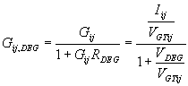
c. Transconductors with degeneration resistors Degenerated transconductors (fig.3.18) can be used to increase the linearity of the input stage. Another positive effect is the increase of the input window of the transconductor. The p version (fig.3.18.a) has larger noise when compared to the T version. The T version (fig.3.18.b) has only one current source. Its noise is a common mode noise and therefore rejected in the differential output. This is paid by a lower efficiency in terms of power due to the voltage drops on the degeneration resistors and the effect of lowering the effective transconductance of the stage. For a degeneration resistor RDEG the equivalent transconductance of the stage becomes smaller due to series feedback. If we denote VDEG the voltage drop on the series resistance RDEG, Gij,DEG the transconductance of the stage and Iij the bias current, then:
Hence, in the DROPT*f0 trade-off the denominator of (3.93) will appear and the effect will be a decrease in the power efficiency. For simplicity assume equal effective gate voltages at saturation onset (VGTij=2nUT). The minimal power in this case can be found from (3.92) and (3.93):
3.6.2. Power estimations for a bandpass filter The power estimation for a biquad can be extended now to the case of a bandpass filter. A bandpass filter with central frequency w0 and the -3dB bandwidth wc is obtained from a low-pass equivalent filter with bandwidth wc by using the biquadratic transformation:
The bandpass filter can be constructed by replacing every integrator in the lowpass filter by an adequate biquad. Given the order of the lowpass prototype n, the order of the bandpass filter is 2n and the number of active elements is 2n. The lowpass filter can be derived from a normalized lowpass filter using the frequency transformation s"=s�/wC. For computing the power, firstly we need to optimize the DR of the filter. According to reference [7], in a bandpass filter derived from a normalized lowpass equivalent filter (in the case of equal capacitance design) the optimal dynamic range follows the inequality:
Optimal DR depends on the maximum effective voltage VM of the transconductor. The frequency w" comes from the normalized lowpass filter which has a noise bandwidth:
In the case of high Q filters, the noise bandwidth can be approximated with 1/p and optimal dynamic range becomes:
The central frequency of the filter w 0 can be considered as the ratio between an equivalent transconductance Geq and the capacitance C. It can be regarded as a linear combination of individual time constants involved in the filter Gi/C.
If the transconductors Gi have input stages biased in strong inversion from a current source Ii then, for a given current efficiency h i we can relate the transconductance to the total current of the filter ITOT:
Hence, the central frequency of the filter becomes:
The trade-off DROPT*f0 as a function of power is found from (3.98) and (3.101):
When all transconductors are biased at VGTi=2nUT the minimum power needed to bias the bandpass filter is found from:
The same discussion can be extrapolated to weak-inversion operation and degenerated transconductors. In conclusion, we have shown how to find the minimal power in the case of a biquad and a bandpass filter. The power involved in this section is the bias power, considering only class A of operation. The minimal power consumption depends on the DROPT*f0 product, the supply voltage, the quality factor of the filter, the noise excess factor of the transconductors, and their current efficiency. It is important to have transconductors with low noise excess factors and high power efficiency capable of large voltage swings with high linearity. The same analysis can be extended to low-pass filter. The difficulty in this case comes from the impossibility to approximate the noise bandwidth from (3.97). |
|
|||||||||||||||||||
|
|
||||||||||||||||||||
|
||||||||||||||||||||

 (3.81)
 (3.88)
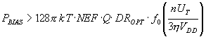 (3.90)
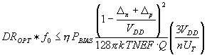
 (3.92.b)
 (3.93)
 (3.94)
 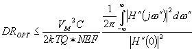 (3.96)
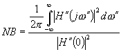 (3.97)
 (3.99)
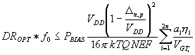 (3.102)
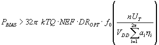 (3.103)


 Animation, 3D Art and 3D Models")