Structured Design Methodology
Last Edit July 22, 2001
Pre-Simulation Steps
Once an array or array series has been selected, the design can be captured
and all checking performed with packaged or vendor software. For non-schematic
designs, the steps leading to the netlist are performed per the system
requirements. Once a netlist exists, the design steps are the same.
Perform schematic capture through netlist generation
-
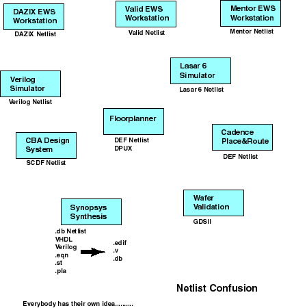
- Perform the schematic capture using the Dazix, Mentor, Valid or other
EWS (Electronic WorkStation) system; Lasar 6, Verilog or other netlister
equipped with schematic-generation software.
Perform the schematic capture following vendor schematic rules and
conventions.
Perform the vendor-software steps through netlist generation
Each workstation has a different netlist format and a different procedure
to generate it. Each workstation has its own simulator that uses the workstation-specific
netlist as an input file. LASAR 6 (Vax/VMS) and Verilog each has a specific
netlist format. Communication of a design from the design workstation
to a vendor must be done using a netlist the array vendor can recognize.
(See Figure 2-2.)
In the 90s, an array vendor was limited to accepting only those designs
created on a workstation that matches the equipment that the vendor has
in-house.
Most design input today is done without schematic capture. Cadence Composer
can handle schematics. Design Compiler from Synopsys will display a schematic
after synthesis (best used at the module level). Today;'s engineers use
Verilog or VHDL netlist to input a circuit description. Design Compiler
produces a Verilog netlist, an EDIF netlist and a Synopsys .db formatted
file for design transfer.
Figure 2-2 Netlister Confusion
Another solution is the use of a dial-up design system based on a mainframe.
The array vendor provides the account access for a fee and provides all
required support and the designer provides an acceptable terminal. The
problem is the access to a compatible terminal when a graphics terminal
is required and the costs of the design in connect time.
To combat the problem of multiple formats without moving to a dial-up
solution, netlist reformatters or translation programs have been written.
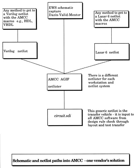
AMCC has a netlist formatter, AGIF, which is customized to each supported
workstation and netlister. The AMCC Generic Interface Format file produced
is called circuit.sdi and it is the means of communication between the
customer and all AMCC software, including the MacroMatrix components:
AMCCERC, AMCCANN, AMCCVRC, AMCCSIMFMT, AMCCSUBMIT and AMCCAD for placement.
Perform design rules checking
For systems and vendors without software support or with support that
is less than complete, the design checks must be performed manually. EWS-based
checking provided by the EWS vendor is minimal and should only be used
as a first step in the validation process. Intelligent checkers are evolving.
These may be interactive with a schematic capture or work on the standardized
netlist.
The checker must be successfully completed before proceeding. Remove
all errors if possible, and document those that remain. The vendor may
require a waiver before submission if errors are not removed from the
circuit.
AMCC customers must run AMCCERC and remove errors. The program output,
AMCCERC.LST, provides reports on population, I/O types and mixes, utilization,
package signal pin requirements, DC power, internal pin count, and SSO
power-ground evaluation while listing naming violations, unconnected pins,
pin connect violations, fan-out loading violations with derated loads,
and technology (array, power-supply, and macro mismatch) errors. AMCCERC.LST
must be included with the design submission package.
Generate extrinsic load time delays (Annotation)
The need for annotation software came from the change in the ratio between
the delays caused by the interconnect between macros and the macro internal
(intrinsic) delays. Once it was common for an interconnect net delay to
exceed one half of the intrinsic delay, or even to exceed the intrinsic
delay, it became necessary to produce a reasonable estimate of the interconnect
delay.
Figure 2-3 Schematic And Netlist Paths Into AMCC
In 2000, the netlist standard had become edif. Verilog, VHD, edif, db,
PDEF are transfer standards now.
Front-Annotation is the term used for pre-placement-pre-route interconnect
delay estimation. The estimate is based on the net size, number of fan-out
loads, both physical and electrical, or the capacitive load on an output
macro.
The Front-Annotation programs such as AMCCANN compute the fan-out loading
delay, the wire-OR loading delay, and provide an estimate of the metal
etch delay due to the size of the nets. The estimate is based on a statistical
evaluation of previously built circuits and the average etch length used
to connect same-sized nets. It is too large a number some of the time
and too small of a number at other times. Front-Annotation is not
a specification.
Where Intermediate-Annotation is available (a Manhattan-Distance algorithm
based on a placement file), it should be used. It is more accurate in
more case but it is still an estimate. Only after place and route can
the actual metal etch delays be known. Annotation after place and route
is called Back-Annotation.
Perform testability analysis on the circuit.
All testability measures have one common goal: to enhance controllability
and observability of the circuit. It is a grade on the logic design itself.
Controllability is a measure of the ease in setting a particular node
to a logic level of zero or one, while observability determines the ease
of propagating the node's state to one or more primary outputs.
After a netlist has been created and logic simulation has verified correct
functional performance, testability can be verified by running testability
analysis programs. This optional step is highly recommended if there is
software available to perform the analysis. For a modular design, a manual
review should be performed if there is no software support.
The purpose is to identify those parts of the circuit that are difficult
or impossible to reach by way of primary inputs (controllability), and
those parts of the circuit that may change state but that are difficult
or impossible to observe at a primary output (observability). Steps should
be taken to make hard to reach nodes controllable by adding test control
signals and degating logic. Make hard to observe nodes observable by adding
test points.
Make any adjustments or changes to the schematic as necessary to improve
testability to acceptable limits. Changing the schematic will mean repeating
the error-checking and annotation software steps.
Testability analysis should be done before simulation since the result
will be to simplify the functional simulation vector set development.
|
