Design Optimization
Last Edit July 22, 2001
Design To Fit The Package
Also at issue at this point in the design stage is the desired package.
When the package is selected, the package methodology for handling added
power and grounds can be determined. Packages can be one-on-one, each
added power and ground pad reaches an external package pin, or they may
have internal power and ground planes.
Not all array pads will reach an internal power or ground plane therefore
there are placement restrictions on the locations of the added power and
ground macros. If these restrictions cannot be met due to other placement
requirements or if the package does not have enough pads that can bond
to internal planes, then the added power or ground macros will require
external package pins. (Example, some packages offer ground planes and
no power planes.)
Case 1 - Count of all array pads less than or equal to the number of
total package pins
There are two approaches to checking the package against the design.
The first is when there are no internal power or ground planes. In this
case, count the number of inputs, outputs, bidirectionals, added power,
added ground, fixed power, fixed ground, and any fixed I/O signals (such
as on-chip thermal diodes and AC speed monitors). This number should be
less than or equal to the total number of package pins.
Case 2 - Count of all signals less than or equal to the number of package
signal pins
The second case involves making an estimate which can be refined after
placement is completed and approved. In this case, count the number of
array pads used by inputs, outputs, bidirectionals, added power, added
ground and any fixed I/O signals such as on-chip thermal diodes or AC
speed monitors. This number should be less than or equal to the total
number of package signal pins. The package power and ground pins connect
to the internal power and ground planes.
After placement, the number of signals will be reduced by the number
of added power and ground macros that were placed to connect to internal
package power and ground planes. Those macros will not use the external
package signal pins.
Example
A designer submitted a design with a desired package (a 149 PGA with
internal power and ground planes). The package has 120 signal pins. He
used 132 array pads for I/O signals and added power and grounds. There
were no fixed thermal diode or AC speed monitor signals on the array.
There were eight added power and grounds. The design, after careful placement
of the added power and grounds, had four signals more than there were
package signal pins.
This problem was not discovered until placement, i.e., until after all
simulations and design validations were performed.
One solution is to look for expendable I/O cell usage. If there are extra
grounds beyond the minimum, or more VBB or other voltage sources than
is really required, they can be reduced.
Another solution is to add an 8:1 MUX, place eight non-critical outputs
as inputs to the MUX, add three input signals to control the select lines
and one output for the MUX. This reduced the total number of signal pins
required to 120, which would fit the package.
What if neither of these solutions is acceptable? Then
some other design change is in order if the package cannot be changed.
A design change requires that all simulations and all checking be repeated.
Could this situation have been prevented? By checking
the package limits during the optimization phase and using the package
limits as a guide, the design changes or package changes could have been
identified earlier, saving the iteration of the simulation loop. Remember
that simulation is estimated to use approximately 50% of the CPU time
used in a design process.
Figure 4-4 Optimization - Packaging Issues
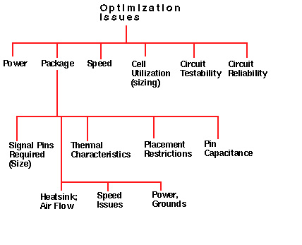
Optimization Issues - Packaging
|
