|
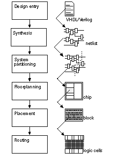
[ Chapter start ] [ Previous page ] [ Next page ] 15.1 Physical DesignFigure 15.1 shows part of the design flow, the physical design steps, for an ASIC (omitting simulation, test, and other logical design steps that have already been covered). Some of the steps in Figure 15.1 might be performed in a different order from that shown. For example, we might, depending on the size of the system, perform system partitioning before we do any design entry or synthesis. There may be some iteration between the different steps too. We must first apply system partitioning to divide a microelectronics system into separate ASICs. In floorplanning we estimate sizes and set the initial relative locations of the various blocks in our ASIC (sometimes we also call this chip planning). At the same time we allocate space for clock and power wiring and decide on the location of the I/O and power pads. Placement defines the location of the logic cells within the flexible blocks and sets aside space for the interconnect to each logic cell. Placement for a gate-array or standard-cell design assigns each logic cell to a position in a row. For an FPGA, placement chooses which of the fixed logic resources on the chip are used for which logic cells. Floorplanning and placement are closely related and are sometimes combined in a single CAD tool. Routing makes the connections between logic cells. Routing is a hard problem by itself and is normally split into two distinct steps, called global and local routing. Global routing determines where the interconnections between the placed logic cells and blocks will be situated. Only the routes to be used by the interconnections are decided in this step, not the actual locations of the interconnections within the wiring areas. Global routing is sometimes called loose routing for this reason. Local routing joins the logic cells with interconnections. Information on which interconnection areas to use comes from the global router. Only at this stage of layout do we finally decide on the width, mask layer, and exact location of the interconnections. Local routing is also known as detailed routing. [ Chapter start ] [ Previous page ] [ Next page ] | |


 Animation, 3D Art and 3D Models")